
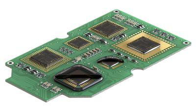
Semiconductor Packaging
Innovative Materials for Evolutionary Electronics Capability
Americas
Asia-Pacific
Europe
South Asia, Middle East & Africa
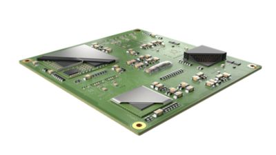
Semiconductor technology and, specifically, the packaging of semiconductor devices has never touched more applications than it does today. As all parts of everyday life become increasingly digitalized – from automobiles to home security to smartphones and 5G infrastructure – semiconductor packaging innovation is at the core of responsive, reliable, robust electronic functionality.
Thinner wafers, decreasing footprints, finer pitches, package integration, 3D designs, wafer-level technology and high-volume production economies of scale demand enabling materials that can support innovation ambitions. Henkel’s total solutions approach leverages extensive global resources to deliver superior semiconductor packaging material technologies and cost-competitive performance. From die attach adhesives used in traditional wirebond packaging to advanced underfills and encapsulants for advanced packaging applications, Henkel provides the cutting-edge materials technology and global support top microelectronics companies require.
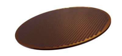
Die Attach Paste
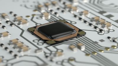
Strong die-to-substrate and die-to-die bonds are the foundation of robust semiconductor packages
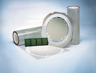
Die Attach Film
Die attach film adhesives have become essential for the production of next-generation semiconductor packages.
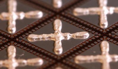
Die Attach: Printable B-Stage
Printable die attach materials provide a viable alternative to standard die attach paste processes, allowing the application of adhesive at the wafer-level.
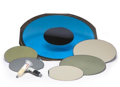
Encapsulation
Protection of ICs, particularly as dimensions continue to shrink and more direct chip attach is incorporated, is critical for long-term semiconductor device reliability.
Underfills
Higher I/O counts, package integration and tighter bump pitches are dictating the use of flip-chip technology to enable advanced package designs.
EMI
The convergence of advanced RF communication capability, miniaturization and package-level integration underscore the requirement for novel approaches to EMI shielding.
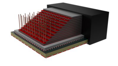
Wafer Level Encapsulation
Wafer-level packaging applications have seen explosive growth as they continue to be key enablers of innovation in mobility products, consumer electronics, data processing and IoT applications, among others.
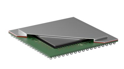
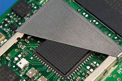
Lid and Stiffener Attach
Advanced flip-chip technology and heterogeneous integration are key enablers of high-performance computing, driving new levels of processing power for desktops, data center servers, autonomous driving systems, and more.
Please fill out the form below and we’ll respond shortly.


