
Wafer-Level Encapsulation
Stability, Protection and Reliability for Wafer-Level Packaging Applications
Americas
Asia-Pacific
Europe
South Asia, Middle East & Africa
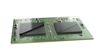
Wafer-level packaging applications have seen explosive growth as they continue to be key enablers of innovation in mobility products, consumer electronics, data processing, and IoT applications, among others. Expansion of functionality within current – or smaller – footprints is driving architectural changes at the wafer level that dictate a need for robust and reliability-enhancing encapsulation materials. Henkel’s portfolio of wafer-level encapsulants offers a variety of solutions to facilitate high-yield processing and in-field reliability for various advanced wafer-level packaging applications.
Wafer-level Packaging
Wafer-level packaging applications have seen explosive growth as they continue to be key enablers of innovation in mobility products, consumer electronics, data processing, and IoT applications, among others.
Wafer Back Side Protection Film
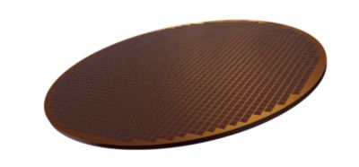
Decreasing dimensions and finer ball pitches of Wafer-Level Chip-Scale Packages (WLCSPs) present handling and processing challenges, particularly as wafers continue to get thinner.
Henkel’s anhydride-free liquid compression molding materials are a REACH-compliant solution for Fan-In and Fan-Out Wafer-Level Packaging (FI WLP and FO WLP) processes. Developed with ultra-fine filler technology (10 µm upper-cut), these unique LOCTITE® brand materials enable very low wafer warpage, deliver void-free fine-dimension gap filling capability, and offer thorough protection for today’s thinner dies. With fast in-mold cure times of five minutes, throughput is accelerated for a high UPH competitive advantage.
As an alternative to compression molding, printable encapsulation materials can be applied at the wafer-level using a standard printing process for wafer-level chip scale packaging applications. Like all wafer-level encapsulation materials in the Henkel portfolio, LOCTITE® printable encapsulants have been formulated to deliver outstanding mechanical and environmental protection for improved reliability in advanced packaging applications. Extremely low wafer warpage, excellent fine-dimension trench-filling capability, good chemical resistance and thermal stability combine to deliver robust protection and stability in a simplified, cost-efficient process.
Decreasing dimensions and finer ball pitches of Wafer-Level Chip-Scale Packages (WLCSPs) present handling and processing challenges, particularly as wafers continue to get thinner. Protecting against die chipping and cracking, warpage, and package damage during the SMT placement process, Henkel’s backside protection (BSP) films help reduce potential mechanical damage. Ideal for miniaturized WLCSP devices measuring < 5.0 mm x 5.0 mm, LOCTITE® BSP films can be supplied in different thickness to accommodate bondline preferences. With good laser marking characteristics, excellent reworkability on 8” and 12” wafers, and ease of processing, Henkel BSP films are low CTE formulations that deliver critical warpage control for improved reliability.
Please fill out the form below and we'll respond shortly.
