
Component Level Electromagnetic Interference (EMI) Shielding Solutions
Reliable shielding and adhesion performance in stressful electronic conditions and environments
Americas
Asia-Pacific
Europe
South Asia, Middle East & Africa
Henkel’s specialized materials, designed to be applied at the package level, have optimal properties and characteristics that provide reliable shielding and adhesion performance in stressful electronic conditions and environments.
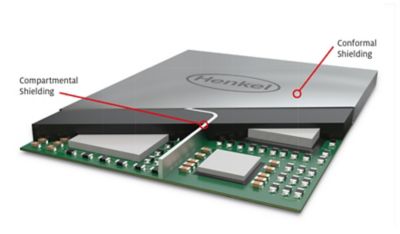
Our compartmental shielding materials portfolio showcases adaptable designs for internal component-to-component shielding with in-package partition, while our conformal shielding materials provide for external package-to-package shielding with an outer coating layer.
Henkel’s flexible material formulations not only mean more reliability and greater functionality, but ensure innovations that deliver more scalable processes, higher production throughput (UPH) and a lower cost of implementation for EMI shielding solutions.
Henkel’s specialized materials, designed to be applied at the package level, have optimal properties and characteristics that provide reliable shielding and adhesion performance in stressful electronic conditions and environments.
Our compartmental shielding materials portfolio showcases adaptable designs for internal component-to-component shielding with in-package partition, while our conformal shielding materials provide for external package-to-package shielding with an outer coating layer.
Henkel’s flexible material formulations not only mean more reliability and greater functionality, but ensure innovations that deliver more scalable processes, higher production throughput (UPH) and a lower cost of implementation for EMI shielding solutions.
With the increasing proliferation of wireless devices, designers are challenged with various electromagnetic waves from multiple sources radiating at the same spectrum of frequencies and resulting in electromagnetic interference (EMI). Radio-frequency (RF) emitting devices require effective isolation to limit the propagation of their interference to neighboring components to protect the end device from performance degradation. As electronics move toward miniaturization, lighter weight, and higher speeds, these challenges become more significant as conventional shielding methods present functional and operational limitations.
Henkel’s specialized materials, designed to be applied at the package level, have optimal properties and characteristics that provide reliable shielding and adhesion performance in stressful electronic conditions and environments.
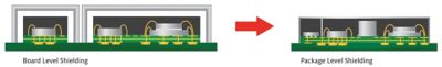
Henkel EMI shielding material technologies enable Faraday cages directly applied at the package level, reducing the dimensions and weight of the overall design and providing a compact and effective shielding method.
Brochure: EMI Shielding Solutions
Please fill out the form below and we'll respond shortly.


